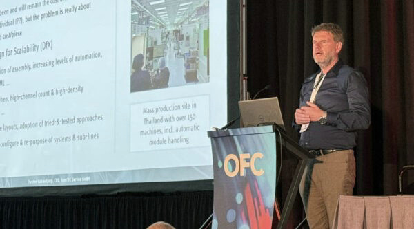
OFC 2024 | ficonTEC:开启集成光子学新篇章,引领未来需求新浪潮
ICC讯 2024年3月在美国圣地亚哥举办的光纤通讯展览会创下了参展商与观展人数新纪录,这标志着在AI技术迅猛发展一年之后,光通讯和网络产业迎来了繁荣和飞速进步的新篇章。
OFC 2024 celebrates unprecedented visitor and exhibitor numbers and spotlights a thriving and rapidly evolving optical communications and networking industry following a year of intensive AI development
通过OFC展,我们见证了一场充满活力且鼓舞人心的技术展示,再次确认了OFC作为全球光通讯和网络行业首屈一指的活动地位。相比2023年,本届展会参展商数量同比增长近四分之一,吸引了约12500名国际观众。展会的焦点议题涵盖了800ZR、相干PON、线性可插拔光学(LPO)、多芯光纤、人工智能(AI)、数据中心技术和量子网络等。
At a very well visited and highly inspiring technology showcase display, OFC 2024 has again solidified the OFC conference’s status as the premier global event for optical networking and communications. With exhibitor numbers up almost a quarter year-on-year and some 12,500 international registered visitors, the most significant focus topics included 800ZR, Coherent PON, Linear Pluggable Optics (LPO), multicore fiber, artificial intelligence (AI), data center technology and quantum networking.
基于集成光子学和相关PIC器件(例如可插拔的CPO共封装光学器件)应用的光学互联技术,已经成为行业重要的技术基石之一—ficonTEC也已在其技术路径上部署了高效的生产设备。然而,由于大规模生成式人工智能网络的需求对市场的直接影响,集成光子学的作用也正在经历一个关键的优先级变化。也就是说,随着市场对数据中心架构组件的需求日益激增,硬件的更新迭代速度也在不断加快。
Optical interconnects based on the utilization of integrated photonics and the associated PIC devices (e.g. in the form of co-packaged optics (CPO) for pluggables) already represent a vital technology cornerstone – a technology approach for which ficonTEC already has active production systems in the field. However, as a direct consequence of a marketplace now propelled by large-scale generative AI network demand, the role of integrated photonics is now undergoing a pivotal change in priority – that is, the surge in interest for the various components that make up data center architecture is also accompanied by an acceleration in the pace of hardware updates.
为了应对这一挑战,关键在于推进集成光子技术的规模化以及提高批量生产能力。而这一点目前还尚未得到充分重视,亟需行业内众多伙伴的紧密协作,共同实现未来光通讯领域原材料、组件、模块和子系统生产的降本增效。
One significant task in catering to this demand will be the scaling of integrated photonics technologies and so too their high-volume manufacturing. This is perhaps currently an underestimated challenge and one that will require close co-operation among multiple partners in the industry to enable the cost-effective manufacturing of materials, components, modules and subsystems for future optical communications.
为了更生动展示行业内直接合作带来的优势,ficonTEC在OFC 2024的展台上还进行了现场演示。并通过和光子封装和工艺开发领域领导者Silitronics Solutions, Inc.(主营业务为光子OSAT即外包半导体封装和测试)的现场合作,生动展示了真实环境下的封装流程。
To showcase the benefits resulting from direct collaboration within the ecosystem, ficonTEC hosted live demos on its booth at OFC 2024. In one example, real-world assembly processes were demonstrated in partnership with Silitronics Solutions, Inc., the leader in photonic packaging and process development as a photonic OSAT (outsourced semi-conductor assembly and test).
Silitronics也充分发挥了ficonTEC制造系统的多项核心竞争力和差异化优势。这些优势源于ficonTEC强大的研发实力及其对制造流程的深刻理解,其中包括可选的基于ML(机器学习)的流程优化工具(ficonEDGE)以及通过虚拟机概念提供培训和“软开发”机会。借助这些工具,在进行协同开发后,初始概念验证原型的周期时间已从20周减少到4周。此外,通过全面的全球化支持、培训项目以及机器重新配置和重新定位选项所带来的灵活性和“工业准备”能力,使这些优势在后期的流程中得到了进一步体现,从而满足不断变化的市场需求和产品迭代。
Silitronics makes use of several competitive differentiators provided by ficonTEC manufacturing systems. The advantages begin with ficonTEC’s unparalleled R&D and experience-driven understanding of manufacturing processes, includes optional ML-based tools for process optimization (ficonEDGE), and provides training and ‘soft development’ opportunities via a virtual machine concept. Using these tools, and after performing collaborative co-development, the cycle time for initial proof-of-concept prototypes has been reduced from 20 to 4 weeks. Moreover, the advantages continue later in one’s own process with comprehensive global support, training programs, and the flexibility and ‘industrial readiness’ provided by machine re-configuration and re-purposing options in order to address evolving market demands and product iterations.
与此同时,Quantifi Photonics还在展会上展示了一系列互补的光子测试解决方案,强调了“为测试而设计”的重要性。这些解决方案包括了激光源、偏振控制器、光功率计和光谱分析仪等设备,它们都是通过精心设计以便能够无缝集成到光电子产品的装配和包装平台。
At the same time, the importance of ‘design-for-test’ was also highlighted on the booth with a range of complementary photonic test solutions exhibited by Quantifi Photonics. This display included laser sources, polarization controllers, optical power meters and optical spectrum analyzers that are all designed to be integrated into assembly and packaging platforms.
展会上,多家企业的联合展示也反映出了光通讯制造技术在未来实际生产中的一些重要要素。首先,随着集成光子学在行业内和其他领域的地位日益凸显,确保组装、测试和封装设备的可重复使用性成为其保持行业先进制造能力的关键要求。与此同时,例如由Silitronics封装解决方案提供的OSAT和合同生产(CM)服务,也展现了在极短的时间内以低成本、高效益模式进行全自动批量生产的能力。最后,Quantify Photonics的测试解决方案解决了在晶圆和/或芯片级别对DUT(被测试设备)进行测试的迫切需求,确保在批量生产环境中光子器件能够全面满足规格要求。该解决方案不但提升了成本效益和测试产量,并支持平行测试,从而优化测试流程。
This type of joint presence at OFC captures some of the all-important aspects of actually manufacturing the optical communication technology of the future. Firstly, in acknowledging the growing role of integrated photonics in this and other sectors, it is clear that assembly, test and packaging equipment must remain reusable in order to retain manufacturing capacity within the respective ecosystems. At the same time, OSAT and contract manufacturing (CM) services provided e.g. by Silitronics’ packaging solutions demonstrate the ability to manufacture flexibly in a fully automated fashion and cost-effectively in high volumes in record times. Finally, Quantifi Photonics’ test solutions address the critical requirement of testing the DUT at the wafer and/or die level, and fully characterizing the photonic devices in volume manufacturing environments to make sure that they meet specifications. The focus is cost-effectiveness and test throughput, and also enabling an optimized test flow with parallel testing where possible.

OFC展会落幕之际,ficonTEC、Silitronics、Quantifi Photonics还与多家行业伙伴包括Global Foundries、Nvidia、Broadcom和Jabil等,共同参加了一场开放性的圆桌讨论。讨论重点是如何在扩大PIC(光集成电路)技术生产规模的同时,保持生产效率和产品质量的领先水平,并分享了提升产量、优化定价策略、缩短生产周期以及保证产品可靠性等方面的经验和见解。
To round out OFC week, ficonTEC, Silitronics and Quantifi Photonics all joined an open panel discussion with other ecosystem companies – including Global Foundries, Nvidia, Broadcom and Jabil – to provide a broader perspective on how to scale PIC technologies for high-volume production with the best yield, pricing, cycle time and quality.
关于ficonTEC
ficonTEC是公认的高端光电子元件和集成光子器件自动化封装和测试设备领域的市场引领者。20多年来,ficonTEC积累了大量的工艺能力和独有的封装技术,可以满足电信/数据通信/5G、高功率二极管激光组装、从生物医学到汽车激光雷达的物联网传感器设备、微光学模块、光纤等行业细分市场的广泛需求。ficonTEC灵活且可扩展的自动化方案,可适用于早期产品开发、新产品导入一直到大批量制造(无论是委约生产还是内部研发和生产)的定制封装和测试解决方案。
ficonTEC is the recognized market leader for automated assembly and testing machine systems for high-end opto-electronic components and integrated photonic devices. Considerable process capability and dedicated assembly technologies have been accumulated over more than two decades of serving the needs of a broad selection of industry segments – including telecom/datacom/5G, high-power diode laser assembly, IoT-conform sensor devices from bio-med to automotive lidar, micro-optical modules, fiber-optics and more. ficonTEC’s flexible and scalable automation options enable customized assembly and test solutions suitable for early device development, for new product introduction (NPI), and all the way up to high-volume manufacturing (HVM) – regardless of whether for contract manufacturing or for in-house R&D and production.
本文地址:http://www.iccsz.com//Site/CN/News/2024/04/22/20240422055607807072.htm 转载请保留文章出处
关键字:
文章标题:OFC 2024 | ficonTEC:开启集成光子学新篇章,引领未来需求新浪潮
2、免责声明,凡本网注明“来源:XXX(非讯石光通讯网)”的作品,均为转载自其它媒体,转载目的在于传递更多信息,并不代表本网赞同其观点和对其真实性负责。因可能存在第三方转载无法确定原网地址,若作品内容、版权争议和其它问题,请联系本网,将第一时间删除。
联系方式:讯石光通讯网新闻中心 电话:0755-82960080-168 Right
- · 光电有约:OFC见闻与市场趋势深析——奇芯光电徐之光先生专访
- · LC:OFC2024是一场人工智能引领所有争议的秀
- · OFC2024官方总结:前所未有的成功 聚焦蓬勃发展的光通信和网络行业
- · OFC2024专访|维度科技:重点展示1.6T/800G测试方案等创新产品方案
- · OFC 2024专访|博升光电:多领域VCSEL顶尖工艺 开放创新一起进步
- · OFC 2024专访|光库科技联合主办薄膜铌酸锂产业论坛 助推商业化进程
- · OFC 2024专访|EXFO:展示先进的测试解决方案,为生成式AI革命铺平道路
- · OFC 2024专访|汇信特:800G相干光波分设备精彩亮相 结合需求带来便捷体验
- · OFC 2024专访|芯泰通信:展出三大类产品 DCI-BOX型OTN传输系统抢眼
- · OFC 2024 精彩回顾 | Hirundo的参展瞬间
- 设置首页 | 光通讯招聘 | 企业搜索库 | 广告服务 | 联系我们 | 保护私隐 | 公司介绍
Copyright ? 2009 ICCSZ.com Inc. All Rights Reserved. 讯石公司 www.iccsz.com版权所有 粤ICP备12008183号-1
